Aside from a stack of Reese’s Peanut Butter Cups, I snagged something else of interest at my Intel meeting at CES 2011: a shot of some exposed Sandy Bridge processor die. As a recap SNB is available in three different physical die versions today: quad-core, dual-core with GT1 graphics and dual-core with GT2 graphics. The die sizes and transistor counts are below:CPU Specification ComparisonCPUManufacturing ProcessCoresTransistor CountDie SizeAMD Thuban 6C45nm6904M346mm2AMD Deneb 4C45nm4758M258mm2Intel Gulftown 6C32nm61.17B240mm2Intel Nehalem/Bloomfield 4C45nm4731M263mm2Intel Sandy Bridge 4C32nm4995M216mm2Intel Lynnfield 4C45nm4774M296mm2Intel Clarkdale 2C32nm2384M81mm2Intel Sandy Bridge 2C (GT1)32nm2504M131mm2Intel Sandy Bridge 2C (GT2)32nm2624M149mm2
Now for the shot:
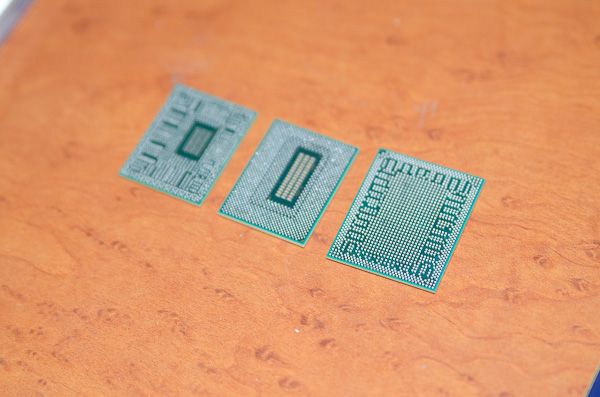
From left to right we have a dual-core GT2 die, a quad-core die and a 32nm Arrandale die with on-package 45nm HD Graphics GPU. There’s very little difference between the dual-core GT2 die and the quad-core die - each SNB core is fairly small at 32nm.
The comparison to Arrandale is also interesting as it makes dual-core SNB look pretty sensible. But keep in mind that we don’t know the full cost structure for manufacturing at 45nm vs. 32nm. Newer processes tend to be more expensive initially compared to older, more mature processes.
]]>
Artikel Terkait:


0 comments:
Post a Comment